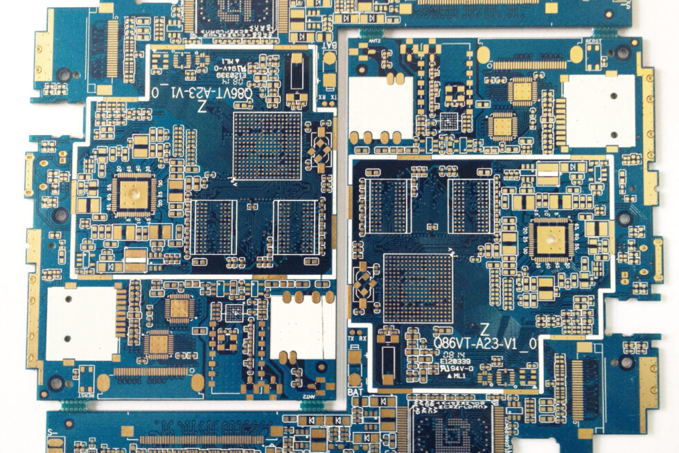
On the same side and in terms of solderability, OSP compared to HASL assembled in the PCA has better performance, but requires the type of flux and the thermal cycling process the number of major changes. Because of its acidic characteristics will reduce the OSP performance, easy oxidation of copper, it requires careful handling. Assembly are more likely to deal with more flexibility and can withstand more heat cycle of the metal surface.
With OSP surface treatment, welding if the test point is not treated will result in the ICT fixture contacts appear needle-bed problem. Only change to adopt a more sharp probe type across the OSP layer will only lead to damage and expose the PCA test vias or test pads. The results show that switching to a higher force or change the detection probe type has little effect on yield. Untreated copper with lead solder are higher than an order of magnitude of the yield strength, the only result is to damage the exposed copper pad test. All testability guidelines are strongly recommended not directly on the bare copper exploration. When using the OSP, the
Need to define a set of OSP rules ICT stage. The most important rule requires the beginning of open technology in PCB version of film (Stencil), to allow the paste can be added to the ICT needs of those who contact pads and vias on the test.
Advantages: in unit costs comparable with HASL, good coplanarity, lead-free technology, to improve weldability.
Cons: assembly process needs major changes, if the detection of unprocessed copper surface is not conducive to ICT, the ICT had a pointed probe may damage the PCB, the preventive treatment need to manually limit the ICT test and reduce test repeatability.
Electroless nickel immersion gold
Electroless nickel immersion gold (ENIG) of this deposited layer in many of the circuit board has been successfully applied, although it has a high unit cost, but it has a smooth surface and excellent solderability. The main disadvantage of electroless nickel layer is very fragile, has been found in the mechanical breakdown under the pressure of the situation. This industry is called “black block” or “mud crack”, which led to some negative reports ENIG.
Advantages: good solderability, flat surface, a long shelf life, can withstand multiple reflow soldering.
Disadvantages: high cost (about 5 times HASL), the “black block” problem, the manufacturing process using cyanide and other harmful chemicals.
Silver Immersion
Immersion silver PCB surface is a latest addition method. Mainly used in Asia, in North America and Europe, gaining promotion.
In the welding process, the silver layer to the solder melting point, in the copper layer to leave a tin / lead / silver alloy, this alloy for the BGA package provides a very reliable solder joints. The contrasting colors make it very easy to check that it is HASL processing in welding a natural alternative.
Immersion silver is a very good development prospects of the surface processing technology, but with all the new technology, like the surface of the end user was very conservative. Many manufacturers of such technology as a “being investigated” the process, but it is likely to be the best lead-free surface of process selection.
Advantages: good solderability, surface roughness, HASL Immersion natural alternative.
Disadvantages: the conservative attitude of end users means that the lack of industry-related information.
Immersion Tin
This is a relatively new surface treatment process, and silver immersion process has many similar characteristics. However, due to the immersion on the PCB manufacturing process through Chengzhong Xi thiourea used (may be a carcinogen) to prevent, so there are significant health and safety issues to consider. In addition, also concerned about the migration of tin (“tin glitch” effect), although the anti-migration of chemicals to control this issue can get some results.
Advantages: good solderability, surface smooth, relatively low cost.
Disadvantages: health and safety issues, limited the number of thermal cycles.
PCB surface treatment summary
The above is the main method of dealing with lead-free PCB. HASL will remain the most widely used PCB treatment process, in which case the test engineer is not changed. In some countries, HASL has been prohibited by law, and using alternatives. With the PCA manufacturing expanded to more different global regions, can be seen in the ICT test lead-free treatment process will be more and more. Although the OSP is not a natural alternative to HASL, but it has become the preferred PCA manufacturers of alternative treatment options. When there is no change in process to allow the test pads and vias on the use of solder paste, this will result in the actual test reliability of ICT
Conclusion, PCB surface treatment process is not perfect, each method has its own issues to be considered. Some of these issues more serious than other problems, all of these lead-free PCB surface treatment process steps need to be modified in order to prevent the emergence in the ICT fixture contact reliability problems.


