Professional PCB Assembly Services: A Full Turnkey Solution from Prototype to Production
GoldenWeald is a leading PCB Assembly (PCBA) service provider, dedicated to delivering high-quality, fast, and cost-effective circuit board manufacturing and assembly solutions for global engineers, startups, and large-scale manufacturers. We specialize in both Surface Mount Technology (SMT) and Through-Hole Technology (THT), handling everything from simple double-sided boards to complex High-Density Interconnect (HDI) layouts.
Why Choose Our PCB Assembly Services?
-
End-to-End Turnkey Solution
-
Complete Peace of Mind: Simply send us your Gerber files, BOM, and centroid data. We manage the entire process: component sourcing, PCB fabrication, precision assembly, comprehensive testing, and final delivery. Our partnerships with leading global component suppliers ensure authentic parts and reliable supply.
-
-
Unmatched Speed and Flexibility
-
Rapid Prototype Assembly: Need a board urgently? We offer quick-turn prototyping in as little as 24 hours to accelerate your development cycle.
-
Low to Mid-Volume Production: Whether your need is 100 or 10,000 units, we provide competitive pricing and stable capacity to seamlessly scale your product from lab to market.
-
-
Advanced Technology & Quality Assurance
-
State-of-the-Art Equipment: Featuring fully automated high-precision SMT pick-and-place machines, multi-zone reflow ovens, AOI (Automated Optical Inspection), X-Ray inspection (for BGA and QFN solder joint verification), and flying probe testers.
-
ISO 9001 Certified: We adhere to strict international quality standards. Every board undergoes multiple inspection checkpoints to ensure a zero-defect delivery.
-
Engineering Support: Our team provides DFM (Design for Manufacturability) analysis to optimize your design before production, saving you cost and improving yield.
-
-
Transparent Pricing & Instant Quotes
-
Use our smart online quoting engine. Upload your files and receive a detailed, transparent quote within minutes—no hidden fees.
-
Our PCB Assembly Capabilities at a Glance
| Service Aspect | Capability Details |
|---|---|
| Assembly Types | Full Turnkey, Partial Turnkey, Consigned (Kitted) |
| Technologies | SMT (01005 components), THT, Mixed Technology, BGA Rework, Conformal Coating |
| Max. PCB Size | 510mm x 460mm |
| Min. Component Size | 0201, 01005 packages |
| BGA Pitch | Supports 0.2mm micro-pitch BGA and CSP |
| Placement Accuracy | ±0.025mm |
| Solder Paste | Lead-Free (RoHS Compliant) or Leaded options |
| Quality Inspection | AOI, X-Ray, First Article Inspection, ICT/FCT |
| Certifications | ISO 9001:2015 |
Industries We Serve
-
Consumer Electronics | Medical Devices | Automotive Electronics | Industrial Controls | Internet of Things (IoT) | Aerospace & Aviation | Telecommunications
Start Your Project in 4 Simple Steps
-
Upload Your Files: Securely upload your Gerber, BOM, and Pick & Place files via our portal.
-
Get an Instant Quote: Our system analyzes your design and generates a detailed quote in minutes.
-
Review & Approve: Confirm your order. Our engineers will perform a complimentary DFM analysis and contact you.
-
Production & Delivery: We manufacture your boards and keep you updated with real-time tracking. Your order is shipped promptly upon completion.
[Get Your Instant Quote Now]
Quote now:
Frequently Asked Questions (FAQ)
Q1: How is the price for PCB assembly calculated?
A: The cost is primarily determined by PCB complexity, component costs, number of solder points, order quantity, and special processes. Use our online quote tool for the most accurate and transparent pricing.
Q2: Do you offer consigned assembly if we provide the components?
A: Yes, we offer full flexibility. You can choose our Full Turnkey service (we source everything) or a Consigned/Kitted model (you provide the components).
Q3: What is your typical turnaround time?
A: For standard prototype orders, turnaround is typically 3-5 business days. The exact time depends on component availability and project complexity. We offer expedited options for faster delivery.
Q4: How do you ensure the reliability of BGA assembly?
A: We ensure BGA reliability through high-accuracy placement and mandatory X-Ray inspection. This allows us to non-destructively check for voids, bridges, and cold joints within the solder balls.
Conclusion: Your Trusted Electronics Manufacturing Partner
Choosing the right PCB assembly manufacturer is critical to the success of your electronic product. With cutting-edge technology, rigorous quality control, and a customer-centric approach, [Your Company Name] is the reliable partner you can count on. Upload your design today and experience a new standard in PCBA service!
[Contact Us] – [View Customer Case Studies] – [Learn More & Resources]
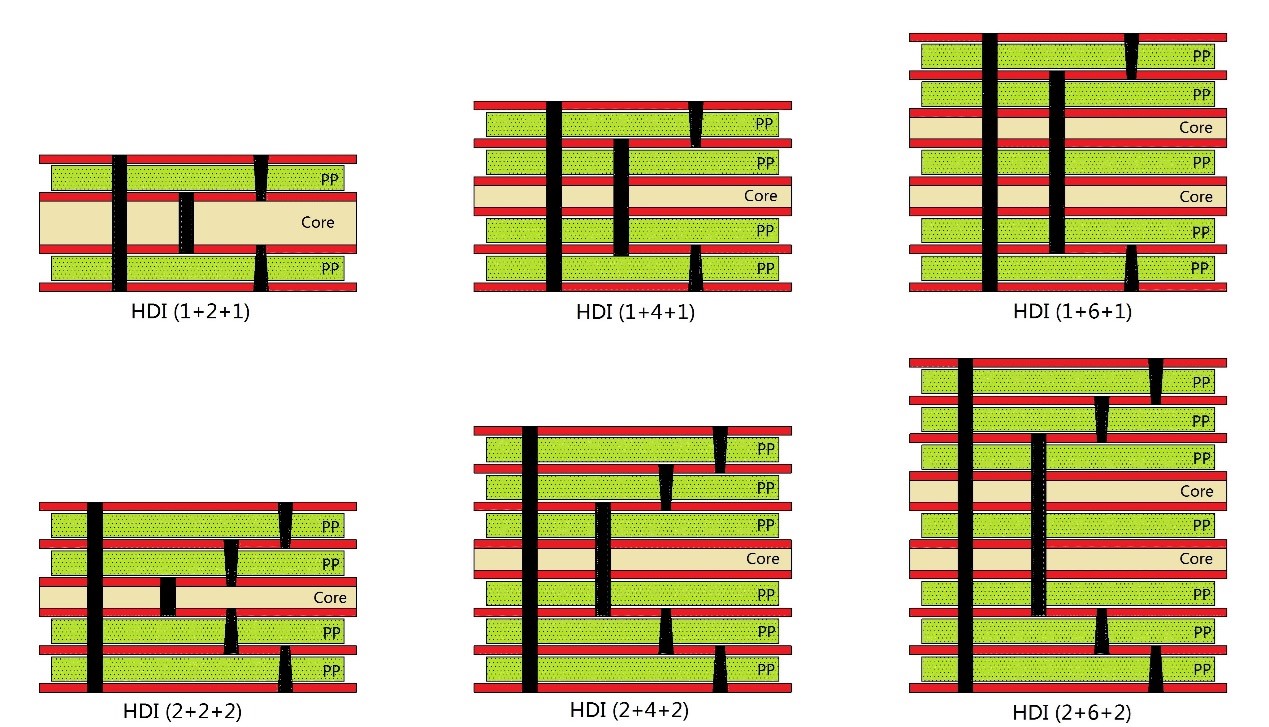
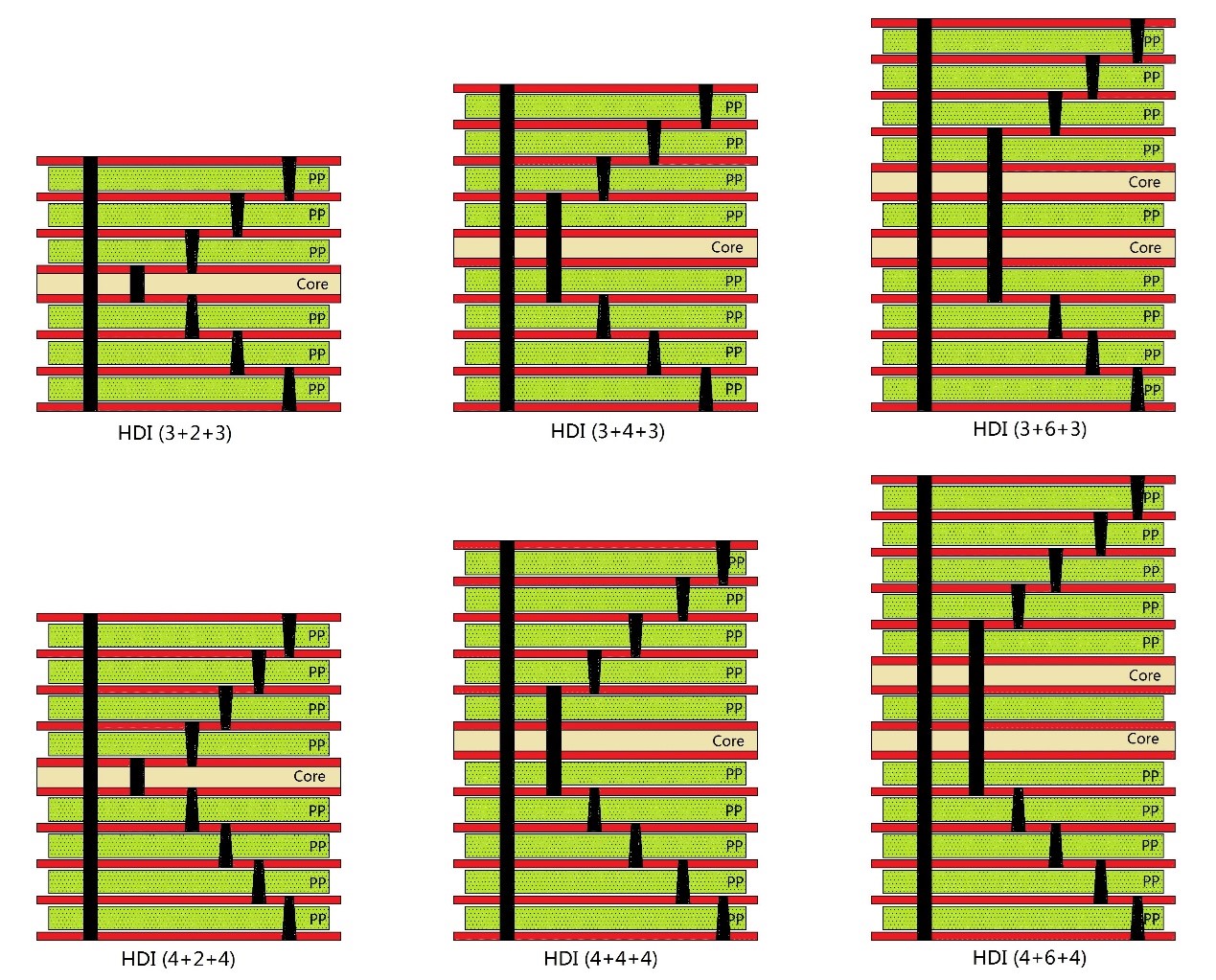
High density interconnect(HDI) PCB, one of the fastest growing technologies in printed circuit boards, have higher circuitry density compared to universal circuit boards. We are committed to providing high quality and reliability HDI printed circuit board manufacturing service to customers with cheap price and quick turnkey.
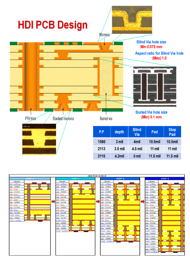

HDI PCBs always contain laser & NC drilling blind vias, buried vias, stack vias, stager vias, skip vias, step vias, through holes, fine lines and spaces, sequential lamination, Via-in-Pad technology and often with microvias diameter not more than 6mil, and etc.
HDI PCB Manufacturing Capacities:
china PCB Assembly, PCB Assembly from china shenzhen Golden Weald Electronic Co., Ltd, 25 years old factory.
| Item | Typical Value | Advanced Production |
| Layer Count | 4-16 Layers | 4-24 Layers |
| PCB Thickness | 0.6-1.0mm | 0.6-3.2mm |
| Buid Up Technology | I+N+I (i≥1) | Any layer innterconnected |
| Min. Laser Drilling Diamter | 4mil (0.1mm) | 3mil (0.075mm) |
| Laser Technology | CO2 Laser Machine | CO2 Laser Machine |
| Glass Transition (Tg) | 130/150/170°C | 130/150/170°C |
| Hole Copper | 12-18μm | 12-18μm |
| Impedance Control | +/-10% | +/-7% |
| Layer to Layer Registration | +/-3mil | +/-2mil |
| Solder Mask Registration | +/-2mil | +/-1mil |
| Min. Trace Width/Spacing | 3/3mil | 2.0/2.0mil |
| Min. Annular Ring | 2.5mil | 2.5mil |
| Min. NC Drilling Diameter | 8mil (0.2mm) | 6mil(0.15mm) |
| Min. Micro Via | 4.0mil | 3.0mil |
| Min. Build-up Dielectric Thickness | 3.0mil | 2.0mil |
| Max. Micro Via Pad | 12mil | 10mil |
| Max. Micro Via Aspect Ratio | 0.8:1 | 1:1 |
HDI Boards Design Rules:
| Item | Capacity | Advanced |
| Base Copper | 9-18μm | 3-18μm |
| Min. Trace Width for Outer Layer | 3mil | 2.5mil |
| Min. Trace Spacing for Outer Layer | 3mil | 3mil |
| Min. Trace Width for Inner Layer | 3mil | 3mil |
| Min. Trace Spacing for Inner Layer | 3mil | 3mil |
| Microvia Size | 4mil (0.1mm) | 3mil(0.075mm) |
| Min. Microvia Landing Pad | Microvia Size + 8mil(0.2mm) | Microvia Size + 6mil(0.15mm) |
| Min. Microvia Pad | Microvia Size + 8mil(0.2mm) | Microvia Size + 8mil(0.2mm) |
| Min. NC Drilling Diameter | 8mil(0.2mm) | 6mil(0.15mm) |
| Min. Pad Size | Drilling Size + 12mil(0.3mm) | Drilling Size + 10mil (0.25mm) |
| Dielectric Thickness | 2-4mil | 2-5mil |
Common used HDI PCB Stackups as below for reference: