Surface-mount components are usually smaller than their counterparts with leads, and are designed to be handled by machines rather than by humans. The electronics industry has standardized package shapes and sizes (the leading standardisation body is JEDEC). These include:
The codes given in the chart below usually tell the length and width of the components in tenths of millimeters or hundredths of inches. For example, a metric 2520 component is 2.5 mm by 2.0 mm which corresponds roughly to .10 inches by .08 inches (hence, imperial size is 1008). Exceptions occur for imperial in the two smallest rectangular passive sizes. The metric codes still represent the dimensions in mm, even though the imperial size codes are no longer aligned. Problematically, some manufacturers are developing metric 0201 components with dimensions of 0.25 mm × 0.125 mm (0.0098 in × 0.0049 in),[7] but the imperial 01005 name is already being used for the 0.4 mm × 0.2 mm (0.0157 in × 0.0079 in) package.

Example of component sizes, metric and imperial codes and comparison included

SMD capacitors (on the left) with two through-hole capacitors (on the right)
- Two-terminal packages
- Rectangular passive components (mostly resistors and capacitors):
- 01005 (0402 metric): 0.4 mm × 0.2 mm (0.0157 in × 0.0079 in). Typical power rating for resistors = 0.031 watt[8]
- 0201 (0603 metric): 0.6 mm × 0.3 mm (0.024 in × 0.012 in). Typical power rating for resistors = 0.05 watt[8]
- 0402 (1005 metric): 1.0 mm × 0.5 mm (0.039 in × 0.020 in). Typical power rating for resistors = 0.1 [8] or 0.062 watt[9]
- 0603 (1608 metric): 1.6 mm × 0.8 mm (0.063 in × 0.031 in). Typical power rating for resistors = 0.1 watt[8]
- 0805 (2012 metric): 2.0 mm × 1.25 mm (0.079 in × 0.049 in). Typical power rating for resistors = 0.125 watt[8]
- 1008 (2520 metric): 2.5 mm × 2.0 mm (0.098 in × 0.079 in). Typical inductor and ferrite bead package[10]
- 1206 (3216 metric): 3.2 mm × 1.6 mm (0.126 in × 0.063 in). Typical power rating for resistors = 0.25 watt[8]
- 1210 (3225 metric): 3.2 mm × 2.5 mm (0.126 in × 0.098 in). Typical power rating for resistors = 0.5 watt[8]
- 1806 (4516 metric): 4.5 mm × 1.6 mm (0.177 in × 0.063 in)[11]
- 1812 (4532 metric): 4.5 mm × 3.2 mm (0.18 in × 0.13 in). Typical power rating for resistors = 0.75 watt[8]
- 2010 (5025 metric): 5.0 mm × 2.5 mm (0.197 in × 0.098 in). Typical power rating for resistors = 0.75 watt[8]
- 2512 (6332 metric): 6.4 mm × 3.2 mm (0.25 in × 0.13 in). Typical power rating for resistors = 1 watt[8]
- 2920: 7.4 mm × 5.1 mm (0.29 in × 0.20 in)[12]
- Tantalum capacitors length (typ.) x width (typ.) x height (max.):[13][14]
- EIA 2012-12 (Kemet R, AVX R): 2.0 mm × 1.3 mm × 1.2 mm
- EIA 3216-10 (Kemet I, AVX K): 3.2 mm × 1.6 mm × 1.0 mm
- EIA 3216-12 (Kemet S, AVX S): 3.2 mm × 1.6 mm × 1.2 mm
- EIA 3216-18 (Kemet A, AVX A): 3.2 mm × 1.6 mm × 1.8 mm
- EIA 3528-12 (Kemet T, AVX T): 3.5 mm × 2.8 mm × 1.2 mm
- EIA 3528-21 (Kemet B, AVX B): 3.5 mm × 2.8 mm × 2.1 mm
- EIA 6032-15 (Kemet U, AVX W): 6.0 mm × 3.2 mm × 1.5 mm
- EIA 6032-28 (Kemet C, AVX C): 6.0 mm × 3.2 mm × 2.8 mm
- EIA 7260-38 (Kemet E, AVX V): 7.3 mm × 6.0 mm × 3.8 mm
- EIA 7343-20 (Kemet V, AVX Y): 7.3 mm × 4.3 mm × 2.0 mm
- EIA 7343-31 (Kemet D, AVX D): 7.3 mm × 4.3 mm × 3.1 mm
- EIA 7343-43 (Kemet X, AVX E): 7.3 mm × 4.3 mm × 4.3 mm
- Aluminium capacitors:[15][16][17]
- (Panasonic / CDE A, Chemi-Con B): 3.3 mm × 3.3 mm
- (Panasonic B, Chemi-Con D): 4.3 mm × 4.3 mm
- (Panasonic C, Chemi-Con E): 5.3 mm × 5.3 mm
- (Panasonic D, Chemi-Con F): 6.6 mm × 6.6 mm
- (Panasonic E/F, Chemi-Con H): 8.3 mm × 8.3 mm
- (Panasonic G, Chemi-Con J): 10.3 mm × 10.3 mm
- (Chemi-Con K): 13.0 mm × 13.0 mm
- (Panasonic H): 13.5 mm × 13.5 mm
- (Panasonic J, Chemi-Con L): 17.0 mm × 17.0 mm
- (Panasonic K, Chemi-Con M): 19.0 mm × 19.0 mm
- SOD: Small Outline Diode
- SOD-723: 1.4 × 0.6 × 0.59 mm [18]
- SOD-523 (SC-79): 1.25 × 0.85 × 0.65 mm [19]
- SOD-323 (SC-90): 1.7 × 1.25 × 0.95 mm [20]
- SOD-128: 5 × 2.7 × 1.1 mm [21]
- SOD-123: 3.68 × 1.17 × 1.60 mm [22]
- SOD-80C: 3.50 × 1.50 × More info [23]
- MELF (Metal Electrode Leadless Face): mostly resistors and diodes; barrel shaped components, dimensions do not match those of rectangular references for identical codes.
- MicroMelf (MMU) Size 0102: length: 2.2 mm, diam.: 1.1 mm. Typical rating for resistors = 0.2 to 0.3 watt / 150 V[24]
- MiniMelf (MMA) Size 0204: length: 3.6 mm, diam.: :1.4 mm. Typical rating for resistors = 0.25 to 0.4 watt / 200 V[24]
- Melf (MMB) Size 0207: length: 5.8 mm, diam.: 2.2 mm. Typical rating for resistors = 0.4 to 1 watt / 300 V[24]
- DO-214
- DO-214AA (SMB): 5.30 × 3.60 × 2.25 mm (Dimension include leads) [25]
- DO-214AB (SMC): 7.95 × 5.90 × 2.25 mm (Dimension include leads) [26]
- DO-214AC (SMA): 5.20 × 2.60 × 2.15 mm (Dimension include leads) [27]
- Rectangular passive components (mostly resistors and capacitors):
- Three-terminal packages
- SOT: Small Outline Transistor, three terminals
- SOT-223: 6.7 mm × 3.7 mm × 1.8 mm body: four terminals, one of which is a large heat-transfer pad [28]
- SOT-89: 4.5 mm × 2.5 mm × 1.5 mm body: four terminals, center pin is connected to a large heat-transfer pad [29]
- SOT-23 (SC-59, TO-236-3): 2.9 mm × 1.3/1.75 mm × 1.3 mm body: three terminals for a transistor [30]
- SOT-323 (SC-70): 2 mm × 1.25 mm × 0.95 mm body: three terminals [31]
- SOT-416 (SC-75): 1.6 mm × 0.8 mm × 0.8 mm body: three terminals [32]
- SOT-663: 1.6 mm × 1.6 mm × 0.55 mm body: three terminals [33]
- SOT-723: 1.2 mm × 0.8 mm × 0.5 mm body: three terminals: flat lead[34]
- SOT-883 (SC-101): 1 mm × 0.6 mm × 0.5 mm body: three terminals: leadless [35]
- DPAK (TO-252, SOT-428): Discrete Packaging. Developed by Motorola to house higher powered devices. Comes in three- or five-terminal versions [36]
- D2PAK (TO-263, SOT-404): bigger than the DPAK; basically a surface mount equivalent of the TO220 through-hole package. Comes in 3, 5, 6, 7, 8 or 9-terminal versions [37]
- D3PAK (TO-268): even larger than D2PAK [38]
- SOT: Small Outline Transistor, three terminals
- Five- and six-terminal packages
- SOT: small-outline transistor, with more than three terminals
- SOT-23-5 (SOT-25, SC-74A): 2.9 mm × 1.3/1.75 mm × 1.3 mm body: five terminals [39]
- SOT-23-6 (SOT-26, SC-74): 2.9 mm × 1.3/1.75 mm × 1.3 mm body: six terminals [40]
- SOT-23-8 (SOT-28): 2.9 mm × 1.3/1.75 mm × 1.3 mm body: eight terminals [41]
- SOT-353 (SC-88A): 2 mm × 1.25 mm × 0.95 mm body: five terminals [42]
- SOT-363 (SC-88, SC-70-6): 2 mm × 1.25 mm × 0.95 mm body: six terminals [43]
- SOT-563: 1.6 mm × 1.2 mm × 0.6 mm body: six terminals [44]
- SOT-665: 1.6 mm × 1.6 mm × 0.55 mm body: six terminals [45]
- SOT-666: 1.6 mm × 1.6 mm × 0.55 mm body: six terminals [46]
- SOT-886: 1.5 mm × 1.05 mm × 0.5 mm body: six terminals: leadless
- SOT-886: 1 mm × 1.45 mm × 0.5 mm body: six terminals: leadless [47]
- SOT-891: 1.05 mm × 1.05 mm × 0.5 mm body: five terminals: leadless
- SOT-953: 1 mm × 1 mm × 0.5 mm body: five terminals
- SOT-963: 1 mm × 1 mm × 0.5 mm body: six terminals
- SOT-1115: 0.9 mm × 1 mm × 0.35 mm body: six terminals: leadless [48]
- SOT-1202: 1 mm × 1 mm × 0.35 mm body: six terminals: leadless [49]
- SOT: small-outline transistor, with more than three terminals
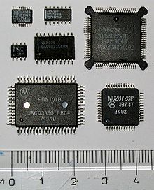
Various SMD chips, desoldered

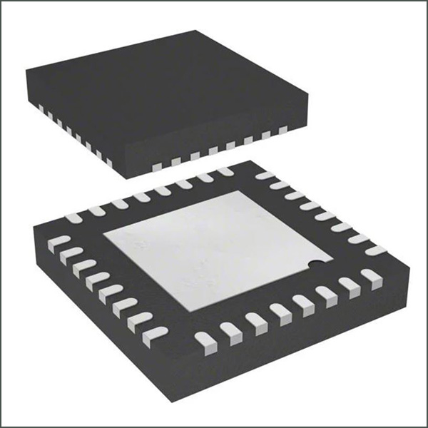
MLP package 28-pin chip, upside down to show contacts

32-pin MQFP chip with manually soldered wires attached for prototyping. The same effect can be achieved using commercially available breakout boards
- Packages with more than six terminals[50]
- Dual-in-line
- flatpack was one of the earliest surface-mounted packages.
- SOIC: (Small-Outline Integrated Circuit), dual-in-line, 8 or more pins, gull-wing lead form, pin spacing 1.27 mm
- SOJ: Small-Outline Package, J-Leaded, the same as SOIC except J-leaded [51]
- TSOP: Thin Small-Outline Package, thinner than SOIC with smaller pin spacing of 0.5 mm
- SSOP: Shrink Small-Outline Package, pin spacing of 0.65 mm, sometimes 0.635 mm or in some cases 0.8 mm
- TSSOP: Thin Shrink Small-Outline package.
- QSOP: Quarter-Size Small-Outline package, with pin spacing of 0.635 mm
- VSOP: Very Small Outline Package, even smaller than QSOP; 0.4, 0.5 mm or 0.65 mm pin spacing
- DFN: Dual Flat No-lead, smaller footprint than leaded equivalent
- Quad-in-line
- PLCC: Plastic Leaded Chip Carrier, square, J-lead, pin spacing 1.27 mm
- QFP: Quad Flat Package, various sizes, with pins on all four sides
- LQFP: Low-profile Quad Flat Package, 1.4 mm high, varying sized and pins on all four sides
- PQFP: Plastic Quad Flat-Pack, a square with pins on all four sides, 44 or more pins
- CQFP: Ceramic Quad Flat-Pack, similar to PQFP
- MQFP: Metric Quad Flat Pack, a QFP package with metric pin distribution
- TQFP: Thin Quad Flat Pack, a thinner version of PQFP
- QFN: Quad Flat No-lead, smaller footprint than leaded equivalent
- LCC: Leadless Chip Carrier, contacts are recessed vertically to “wick-in” solder. Common in aviation electronics because of robustness to mechanical vibration.
- MLP (MLF): Micro Leadframe Package (Micro Lead-Frame package) with a 0.5 mm contact pitch, no leads (same as QFN) [52]
- PQFN: Power Quad Flat No-lead, with exposed die-pad[s] for heatsinking
- Grid arrays
- PGA: Pin grid array.
- BGA: Ball Grid Array, with a square or rectangular array of solder balls on one surface, ball spacing typically 1.27 mm
- LGA: An array of bare lands only. Similar to in appearance to QFN, but mating is by spring pins within a socket rather than solder.
- FBGA: Fine pitch Ball Grid Array, with a square or rectangular array of solder balls on one surface
- LFBGA: Low profile Fine pitch Ball Grid Array, with a square or rectangular array of solder balls on one surface, ball spacing typically 0.8 mm
- TFBGA: Thin Fine pitch Ball Grid Array, with a square or rectangular array of solder balls on one surface, ball spacing typically 0.5 mm
- CGA: Column Grid Array, circuit package in which the input and output points are high temperature solder cylinders or columns arranged in a grid pattern.
- CCGA: Ceramic Column Grid Array, circuit package in which the input and output points are high temperature solder cylinders or columns arranged in a grid pattern. The body of the component is ceramic.
- μBGA: micro-BGA, with ball spacing less than 1 mm
- LLP: Lead Less Package, a package with metric pin distribution (0.5 mm pitch).
- Non-packaged devices (although surface-mount, these devices require specific process for assembly):
- COB: Chip-On-Board; a bare silicon chip, that is usually an integrated circuit, is supplied without a package (usually a lead frame overmolded with epoxy) and is attached, often with epoxy, directly to a circuit board. The chip is then wire bonded and protected from mechanical damage and contamination by an epoxy “glob-top”.
- COF: Chip-On-Flex; a variation of COB, where a chip is mounted directly to a flex circuit.
- COG: Chip-On-Glass; a variation of COB, where a chip, typically a Liquid crystal display (LCD) controller, is mounted directly on glass:.
- Dual-in-line
There are often subtle variations in package details from manufacturer to manufacturer, and even though standard designations are used, designers need to confirm dimensions when laying out printed circuit boards.
Identification
Resistors
For 5% precision SMD resistors usually are marked with their resistance values using three digits, two significant digits and a multiplier digit. These are quite often white lettering on a black background, but other colored backgrounds and lettering can be used.
The black or colored coating is usually only on one face of the device, the sides and other face simply being the uncoated, usually white ceramic substrate. The coated surface, with the resistive element beneath is normally positioned face up when the device is soldered to the board although they can rarely be seen mounted with the uncoated underside face up, whereby the resistance value code is not visible.
For 1% precision SMD resistors, the EIA-96 code is used, as three digits would otherwise not convey enough information. This code consists of two digits and a letter: the digits denote the value’s position in the E96 sequence, while the letter indicates the multiplier.Typical examples of resistance codes102 = 10 00 = 1,000 Ω = 1 kΩ0R2 = 0.2 Ω684 = 68 0000 = 680,000 Ω = 680 kΩ68X = 499 × 0.1 = 49.9 Ω[53]
There is an online tool to translate codes to resistance values on the Hobby-Hour website. resistors can be found in several types of material but the most common is ceramic resistor where the substrate is ceramic. value are available in several tolerances defined in EIA Decade Values Table :
E3 50% tolerance (no longer used)
E6 20% tolerance (now seldom used)
E12 10% tolerance
E24 5% tolerance
E48 2% tolerance
E96 1% tolerance
E192 0.5, 0.25, 0.1% and higher tolerances
Capacitors
Non electrolytic capacitors are usually unmarked and the only reliable method of determining their value is removal from the circuit and subsequent measurement with a capacitance meter or impedance bridge. The materials used to fabricate the capacitors, such as Nickel Tantalate, possess different colours and these can give an approximate idea of the capacitance of the component.Light grey body colour indicates a capacitance which is generally less than 100 pF.Medium Grey colour indicates a capacitance anywhere from 10 pF to 10 nF.Light brown colour indicates a capacitance in a range from 1 nF to 100 nF.Medium brown colour indicates a capacitance in a range from 10 nF to 1 μF.Dark brown colour indicates a capacitance from 100 nF to 10 μF.Dark grey colour indicates a capacitance in the μF range, generally 0.5 to 50 μF, or the device may be an inductor and the dark grey is the color of the ferrite bead. (An inductor will measure a low resistance to a multimeter on the resistance range whereas a capacitor, out of the circuit, will measure a near infinite resistance.)
Generally physical size is proportional to capacitance and voltage^2 for the same dielectric. For example, a 100 nF 50 V capacitor may come in the same package as a 10 nF 150 V device.
SMD (non electrolytic) capacitors, which are usually monolithic ceramic capacitors, exhibit the same body color on all four faces not covered by the end caps.
SMD electrolytic capacitors, usually tantalum capacitors, and film capacitors are marked like resistors, with two significant figures and a multiplier in units of pico Farads or pF, (10−12 Farad.)Examples104 = 100 nF = 100,000 pF226 = 22 μF = 22,000,000 pF
The electrolytic capacitors are usually encapsulated in black or beige epoxy resin with flat metal connecting strips bent underneath. Some film or tantalum electrolytic types are unmarked and possess red, orange or blue body colors with complete end caps, not metal strips.
Inductors
Due to the small dimensions of SMDs, SMT inductors are limited to values of less than about 10 mH.Smaller inductance with moderately high current ratings are usually of the ferrite bead type. They are simply a metal conductor looped through a ferrite bead and almost the same as their through-hole versions but possess SMD end caps rather than leads. They appear dark grey and are magnetic, unlike capacitors with a similar dark grey appearance. These ferrite bead type are limited to small values in the nH (nano Henry), range and are often used as power supply rail decouplers or in high frequency parts of a circuit. Larger inductors and transformers may of course be through-hole mounted on the same board.
SMT inductors with larger inductance values often have turns of wire or flat strap around the body or embedded in clear epoxy, allowing the wire or strap to be seen. Sometimes a ferrite core is present also. These higher inductance types are often limited to small current ratings, although some of the flat strap types can handle a few amps.
As with capacitors, component values and identifiers are not usually marked on the component itself; if not documented or printed on the PCB, measurement, usually removed from the circuit, is the only way of determining them.
Discrete semiconductors
Discrete semiconductors, such as transistors, diodes and F.E.T.s are often marked with a two- or three-symbol code in which the same code marked on different packages or on devices made by different manufacturers can translate to different devices.
Many of these codes, used because the devices are too small to be marked with more traditional numbers used on through-hole equivalent devices, correlate to more familiar traditional part numbers when a correlation list is consulted.
GM4PMK in the United Kingdom has prepared a correlation list, and a similar .pdf list is also available, although these lists are not complete.
Integrated circuits
Generally, integrated circuit packages are large enough to be imprinted with the complete part number which includes the manufacturer’s specific prefix, or a significant segment of the part number and the manufacturer’s name or logo.Examples of manufacturers’ specific prefixes:
- Philips HEF4066 or Motorola MC14066. (a 4066 Quad Analog Switch.)
- Fujitsu Electric FA5502. (a 5502M Boost Architecture Power factor correction controller.)


1 Comment
video
Thiss iis mmy first ime ggo to see aat hre and i am really mpressed to rread evertrhing at siingle place.