Surface-mount technology (SMT) is a method for producing electronic circuits in which the components are mounted or placed directly onto the surface of printed circuit boards (PCBs). An electronic device so made is called a surface-mount device (SMD). In the industry it has largely replaced the through-hole technology construction method of fitting components with wire leads into holes in the circuit board. Both technologies can be used on the same board for components not suited to surface mounting such as large transformers and heat-sinked power semiconductors.
An SMT component is usually smaller than its through-hole counterpart because it has either smaller leads or no leads at all. It may have short pins or leads of various styles, flat contacts, a matrix of solder balls (BGAs), or terminations on the body of the component.
History
Surface mounting was originally called “planar mounting”.[1]
Surface-mount technology was developed in the 1960s and became widely used in the late 1980s. Much of the pioneering work in this technology was by IBM. The design approach first demonstrated by IBM in 1960 in a small-scale computer was later applied in the Launch Vehicle Digital Computer used in the Instrument Unit that guided all Saturn IB and Saturn V vehicles.[2] Components were mechanically redesigned to have small metal tabs or end caps that could be directly soldered to the surface of the PCB. Components became much smaller and component placement on both sides of a board became far more common with surface mounting than through-hole mounting, allowing much higher circuit densities. Often only the solder joints hold the parts to the board, in rare cases parts on the bottom or “second” side of the board may be secured with a dot of adhesive to keep components from dropping off inside reflow ovens if the part has a large size or weight.Adhesive is sometimes used to hold SMT components on the bottom side of a board if a wave soldering process is used to solder both SMT and through-hole components simultaneously. Alternatively, SMT and through-hole components can be soldered together without adhesive if the SMT parts are first reflow-soldered, then a selective solder mask is used to prevent the solder holding the parts in place from reflowing and the parts floating away during wave soldering. Surface mounting lends itself well to a high degree of automation, reducing labor cost and greatly increasing production rates. SMDs can be one-quarter to one-tenth the size and weight, and one-half to one-quarter the cost of equivalent through-hole parts.
Terms
Because “surface-mount” refers to a methodology of manufacturing, there are different terms used when referring to the different aspect of the method, which distinguishes for example the components, technique, and machines used in manufacturing. These terms are listed in the following table:
| SMp term | Expanded form |
|---|---|
| SMD | Surface-mount devices (active, passive and electromechanical components) |
| SMT | Surface-mount technology (assembling and mounting technology) |
| SMA | Surface-mount assembly (module assembled with SMT) |
| SMC | Surface-mount components (components for SMT) |
| SMP | Surface-mount packages (SMD case forms) |
| SME | Surface-mount equipment (SMT assembling machines) |
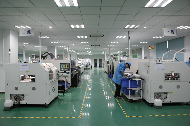
Assembly techniques

Assembly line with SMT placement machines
Where components are to be placed, the printed circuit board normally has flat, usually tin-lead, silver, or gold plated copper pads without holes, called solder pads. Solder paste, a sticky mixture of flux and tiny solder particles, is first applied to all the solder pads with a stainless steel or nickel stencil using a screen printing process. It can also be applied by a jet-printing mechanism, similar to an inkjet printer. After pasting, the boards then proceed to the pick-and-place machines, where they are placed on a conveyor belt. The components to be placed on the boards are usually delivered to the production line in either paper/plastic tapes wound on reels or plastic tubes. Some large integrated circuits are delivered in static-free trays. Numerical control pick-and-place machines remove the parts from the tapes, tubes or trays and place them on the PCB.
The boards are then conveyed into the reflow soldering oven. They first enter a pre-heat zone, where the temperature of the board and all the components is gradually, uniformly raised. The boards then enter a zone where the temperature is high enough to melt the solder particles in the solder paste, bonding the component leads to the pads on the circuit board. The surface tension of the molten solder helps keep the components in place, and if the solder pad geometries are correctly designed, surface tension automatically aligns the components on their pads. There are a number of techniques for reflowing solder. One is to use infrared lamps; this is called infrared reflow. Another is to use a hot gas convection. Another technology which is becoming popular again is special fluorocarbon liquids with high boiling points which use a method called vapor phase reflow. Due to environmental concerns, this method was falling out of favor until lead-free legislation was introduced which requires tighter controls on soldering. Currently, at the end of 2008, convection soldering is the most popular reflow technology using either standard air or nitrogen gas. Each method has its advantages and disadvantages. With infrared reflow, the board designer must lay the board out so that short components don’t fall into the shadows of tall components. Component location is less restricted if the designer knows that vapor phase reflow or convection soldering will be used in production. Following reflow soldering, certain irregular or heat-sensitive components may be installed and soldered by hand, or in large-scale automation, by focused infrared beam (FIB) or localized convection equipment.
If the circuit board is double-sided then this printing, placement, reflow process may be repeated using either solder paste or glue to hold the components in place. If a wave soldering process is used, then the parts must be glued to the board prior to processing to prevent them from floating off when the solder paste holding them in place is melted.
After soldering, the boards may be washed to remove flux residues and any stray solder balls that could short out closely spaced component leads. Rosin flux is removed with fluorocarbon solvents, high flash point hydrocarbon solvents, or low flash solvents e.g. limonene (derived from orange peels) which require extra rinsing or drying cycles. Water soluble fluxes are removed with deionized water and detergent, followed by an air blast to quickly remove residual water. However, most electronic assemblies are made using a “No-Clean” process where the flux residues are designed to be left on the circuit board [benign]. This saves the cost of cleaning, speeds up the manufacturing process, and reduces waste.
Certain manufacturing standards, such as those written by the IPC – Association Connecting Electronics Industries require cleaning regardless of the solder flux type used to ensure a thoroughly clean board. Even no-clean flux leaves a residue which, under IPC standards, must be removed.[citation needed] Proper cleaning removes all traces of solder flux, as well as dirt and other contaminants that may be invisible to the naked eye. However, while shops conforming to IPC standard are expected to adhere to the Association’s rules on board condition, not all manufacturing facilities apply IPC standard, nor are they required to do so. Additionally, in some applications, such as low-end electronics, such stringent manufacturing methods are excessive both in expense and time required.
Finally, the boards are visually inspected for missing or misaligned components and solder bridging. If needed, they are sent to a rework station where a human operator repairs any errors. They are then usually sent to the testing stations (in-circuit testing and/or functional testing) to verify that they operate correctly.
Advantages
The main advantages of SMT over the older through-hole technique are:
- Smaller components. As of 2012 smallest was 0.4 × 0.2 mm (0.016 × 0.008 in: 01005). Expected to sample in 2013 are 0.25 × 0.125 mm (0.010 × 0.005 in, size not yet standardized)
- Much higher component density (components per unit area) and many more connections per component.
- Lower initial cost and time of setting up for production.
- Fewer holes need to be drilled.
- Simpler and faster automated assembly. Some placement machines are capable of placing more than 136,000 components per hour.
- Small errors in component placement are corrected automatically as the surface tension of molten solder pulls components into alignment with solder pads.
- Components can be placed on both sides of the circuit board.
- Lower resistance and inductance at the connection; consequently, fewer unwanted RF signal effects and better and more predictable high-frequency performance.
- Better mechanical performance under shake and vibration conditions.
- Many SMT parts cost less than equivalent through-hole parts.
- Better EMC performance (lower radiated emissions) due to the smaller radiation loop area (because of the smaller package) and the smaller lead inductance.[3]
Disadvantages
- Manual prototype assembly or component-level repair is more difficult and requires skilled operators and more expensive tools, due to the small sizes and lead spacings of many SMDs.
- SMDs cannot be used directly with plug-in breadboards (a quick snap-and-play prototyping tool), requiring either a custom PCB for every prototype or the mounting of the SMD upon a pin-leaded carrier. For prototyping around a specific SMD component, a less-expensive breakout board may be used. Additionally, stripboard style protoboards can be used, some of which include pads for standard sized SMD components. For prototyping, “dead bug” breadboarding can be used.[4]
- SMDs’ solder connections may be damaged by potting compounds going through thermal cycling.
- Solder joint dimensions in SMT quickly become much smaller as advances are made toward ultra-fine pitch technology. The reliability of solder joints becomes more of a concern, as less and less solder is allowed for each joint. Voiding is a fault commonly associated with solder joints, especially when reflowing a solder paste in the SMT application. The presence of voids can deteriorate the joint strength and eventually lead to joint failure.[5][6]
- SMT is unsuitable for large, high-power, or high-voltage parts, for example in power circuitry. It is common to combine SMT and through-hole construction, with transformers, heat-sinked power semiconductors, physically large capacitors, fuses, connectors, and so on mounted on one side of the PCB through holes.
- SMT is unsuitable as the sole attachment method for components that are subject to frequent mechanical stress, such as connectors that are used to interface with external devices that are frequently attached and detached.
Rework

Removal of surface-mount device using soldering tweezers
Main article: rework (electronics)
Defective surface-mount components can be repaired by using soldering irons (for some connections), or using a non-contact rework system. In most cases a rework system is the better choice because SMD work with a soldering iron requires considerable skill, and is not always feasible. There are essentially two non-contact soldering/desoldering methods: infrared soldering and soldering with hot gas.
Infrared
With infrared soldering, the energy for heating up the solder joint is transmitted by long- or short-wave infrared electromagnetic radiation.
Benefits:
- Easy setup
- No compressed air required
- No requirement for different nozzles for many component shapes and sizes, reducing cost and the need to change nozzles
- Fast reaction of infrared source (depends on system used)
Disadvantages:
- Central areas will be heated more than peripheral areas
- Temperature control is less precise, and there may be peaks
- Nearby components must be shielded from heat to prevent damage, which requires additional time for every board
- Surface temperature depends on the component’s albedo: dark surfaces will be heated more than lighter surfaces
- The temperature additionally depends on the surface shape. Convective loss of energy will reduce the temperature of the component
- No reflow atmosphere possible
Hot gas
During hot gas soldering, the energy for heating up the solder joint is transmitted by a hot gas. This can be air or inert gas (nitrogen).
Benefits:
- Simulating reflow oven atmosphere
- Some systems allow switching between hot air and nitrogen
- Standard and component-specific nozzles allow high reliability and faster processing
- Allow reproducible soldering profiles
- Efficient heating, large amounts of heat can be transferred
- Even heating of the affected board area
- Temperature of the component will never exceed the adjusted gas temperature
- Rapid cooling after reflow, resulting in small-grained solder joints (depends on system used)
Disadvantages:
- Thermal capacity of the heat generator results in slow reaction whereby thermal profiles can be distorted (depends on system used)
Reworking usually corrects some type of error, either human- or machine-generated, and includes the following steps:
- Melt solder and remove component (s)
- Remove residual solder
- Print solder paste on PCB, directly or by dispensing
- Place new component and reflow.
Sometimes hundreds or thousands of the same part need to be repaired. Such errors, if due to assembly, are often caught during the process. However, a whole new level of rework arises when component failure is discovered too late, and perhaps unnoticed until the end user of the device being manufactured experiences it. Rework can also be used if products of sufficient value to justify it require revision or re-engineering, perhaps to change a single firmware-based component. Reworking in large volume requires an operation designed for that purpose.

