High density interconnect(HDI) PCB, one of the fastest growing technologies in printed circuit boards, have higher circuitry density compared to universal circuit boards. We are committed to providing high quality and reliability HDI printed circuit board manufacturing service to customers with cheap price and quick turnkey.

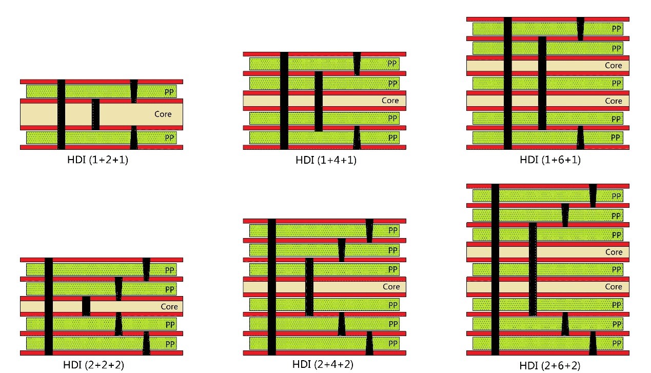
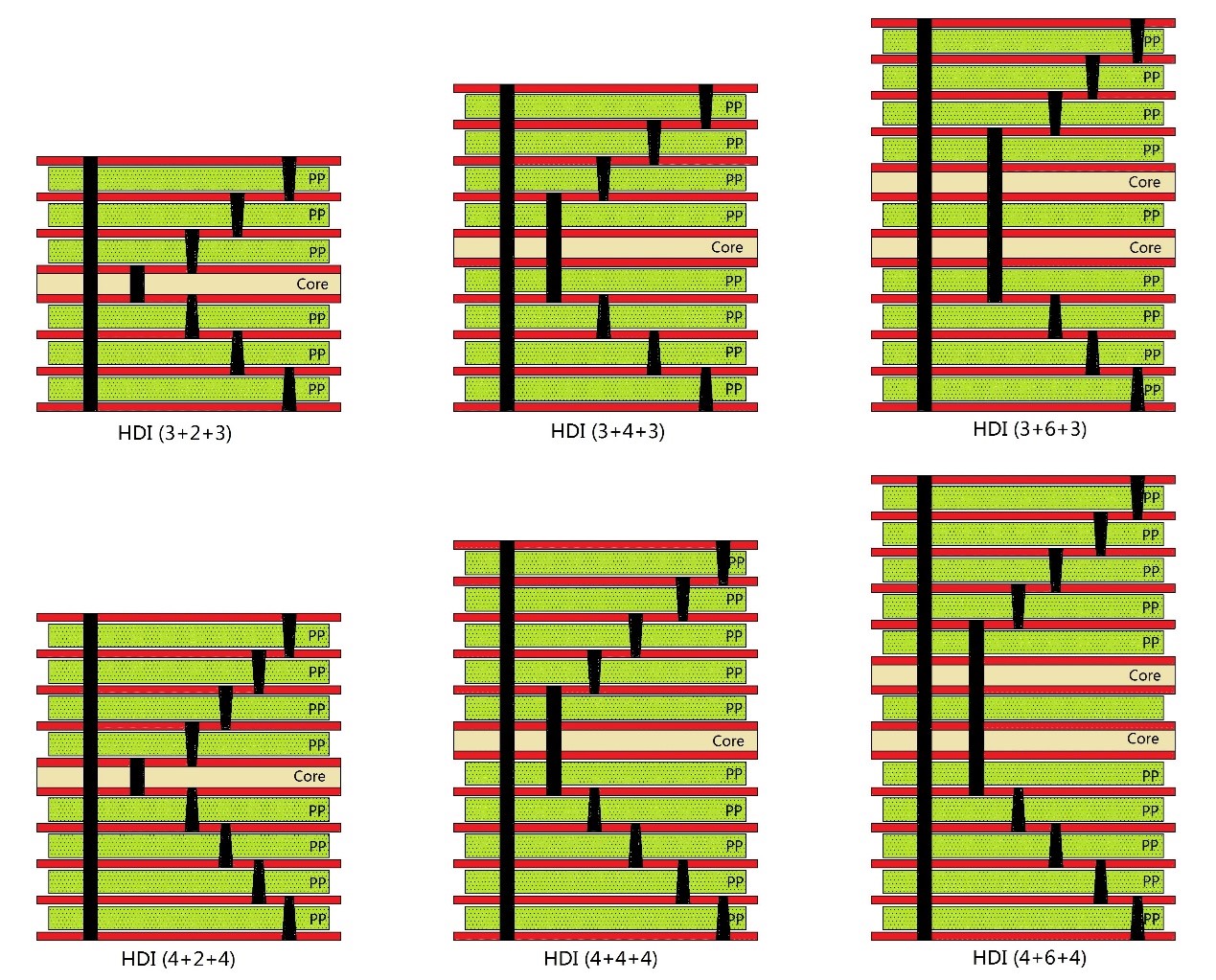
HDI PCBs always contain laser & NC drilling blind vias, buried vias, stack vias, stager vias, skip vias, step vias, through holes, fine lines and spaces, sequential lamination, Via-in-Pad technology and often with microvias diameter not more than 6mil, and etc.
HDI PCB Manufacturing Capacities:
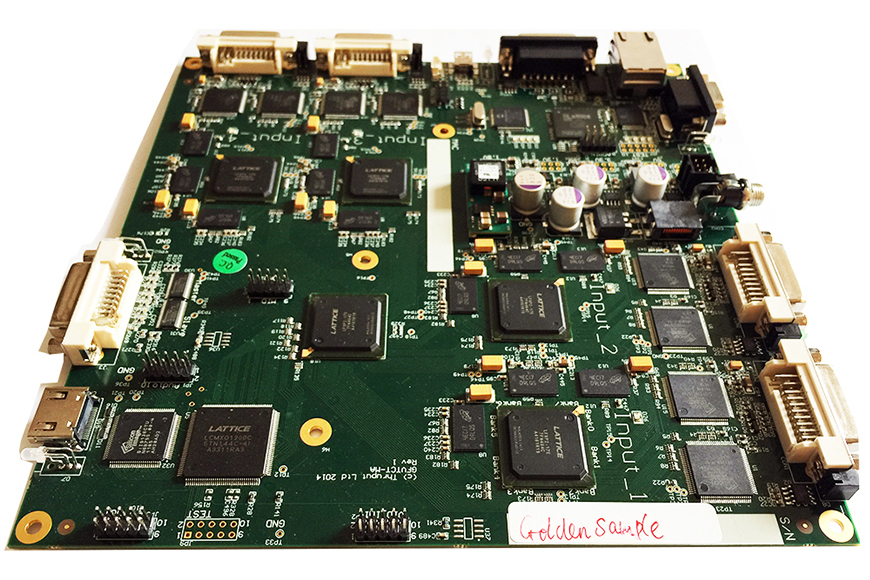
china PCB Assembly, PCB Assembly from china shenzhen Golden Weald Electronic Co., Ltd, 25 years old factory.
| Item | Typical Value | Advanced Production |
| Layer Count | 4-16 Layers | 4-24 Layers |
| PCB Thickness | 0.6-1.0mm | 0.6-3.2mm |
| Buid Up Technology | I+N+I (i≥1) | Any layer innterconnected |
| Min. Laser Drilling Diamter | 4mil (0.1mm) | 3mil (0.075mm) |
| Laser Technology | CO2 Laser Machine | CO2 Laser Machine |
| Glass Transition (Tg) | 130/150/170°C | 130/150/170°C |
| Hole Copper | 12-18μm | 12-18μm |
| Impedance Control | +/-10% | +/-7% |
| Layer to Layer Registration | +/-3mil | +/-2mil |
| Solder Mask Registration | +/-2mil | +/-1mil |
| Min. Trace Width/Spacing | 3/3mil | 2.0/2.0mil |
| Min. Annular Ring | 2.5mil | 2.5mil |
| Min. NC Drilling Diameter | 8mil (0.2mm) | 6mil(0.15mm) |
| Min. Micro Via | 4.0mil | 3.0mil |
| Min. Build-up Dielectric Thickness | 3.0mil | 2.0mil |
| Max. Micro Via Pad | 12mil | 10mil |
| Max. Micro Via Aspect Ratio | 0.8:1 | 1:1 |
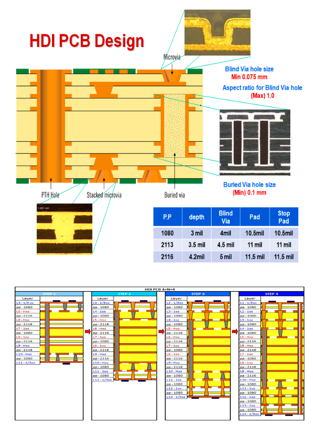
HDI Boards Design Rules:
| Item | Capacity | Advanced |
| Base Copper | 9-18μm | 3-18μm |
| Min. Trace Width for Outer Layer | 3mil | 2.5mil |
| Min. Trace Spacing for Outer Layer | 3mil | 3mil |
| Min. Trace Width for Inner Layer | 3mil | 3mil |
| Min. Trace Spacing for Inner Layer | 3mil | 3mil |
| Microvia Size | 4mil (0.1mm) | 3mil(0.075mm) |
| Min. Microvia Landing Pad | Microvia Size + 8mil(0.2mm) | Microvia Size + 6mil(0.15mm) |
| Min. Microvia Pad | Microvia Size + 8mil(0.2mm) | Microvia Size + 8mil(0.2mm) |
| Min. NC Drilling Diameter | 8mil(0.2mm) | 6mil(0.15mm) |
| Min. Pad Size | Drilling Size + 12mil(0.3mm) | Drilling Size + 10mil (0.25mm) |
| Dielectric Thickness | 2-4mil | 2-5mil |
Common used HDI PCB Stackups as below for reference: